Hardware of LCQ-Meter
The LCQ-Meter – a Microcontroller Based Implementation
After all that theory let’s see how this is actually implemented in the LCQ-Meter. Picture 9 shows the different components at an overview level.
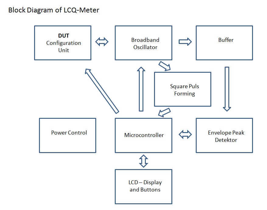
Picture 9: Block diagram of the LCQ-Meter
A modern but affordable microcontroller from Microchip, the 16F1788 takes over all the control, display and input processing.
The DUT Configuration Unit is a relay switched network which allows to combine internal fixed and reference capacitors, an internal inductor and the DUT L, C or LC tuned circuit in different serial and parallel configurations for the different measurement modes. Finally in each configuration the result is an LC parallel tuned circuit to act as the frequency describing element for the Broadband Oscillator.
The Broadband Oscillator can be switched on and off by the microcontroller. There is also a capability to kick the oscillator to ensure starting swinging. The oscillator is described in the next paragraph in detail.
For frequency measurement (internal and external) a Square Pulse Former converts the signal from the oscillator to a clean square pulse. This is needed as the microcontroller can only count clean square pulses on a reliable base.
For quality measurement the oscillator will be periodically switched off. To attenuate the tuned circuit as less as possible during envelope measurement a high efficiency buffer is placed before the Envelope Peak Detector.
The Envelope Peak Detector can be switched on and off by the microcontroller to allow measurement of the envelope at a specific time. This unit will be described in detail in one of the next paragraphs.
There is also a little bit effort needed for voltage regulation, bypassing etc. This is covered by the Power Control Block. In the current version the LCQ-Meter can be run by 3 different power sources including 2 - 3 AA size batteries to make it a portable unit.
Broadband Amplitude Stabilized Oscillator
The Broadband Amplitude Stabilized Oscillator, together with the Peak Detector, are the most challenging components of the overall design.
Several requirements have to be met:
1. The oscillator has to cover multiple decades of frequency without component change. Measuring tuned circuits of mH and nF means oscillation at some 10 KHz, measuring tuned circuits of uH and pF means oscillation at some 10 MHz.
2. The oscillator has to oscillate with relatively high, if possible constant amplitude to allow envelope measurement without any needed additional amplification or gain control.
3. The oscillator has to allow a parallel tuned circuit to be the only frequency relevant element.
4. The oscillator has to be on and off switchable without attenuating the tuned circuit element after being switched off. Also no relevant extra current has to be introduced during off switching to avoid spikes.
5. The oscillator has to be ESD save. Attaching a capacitor, inductor or a tuned circuit as the DUT should not kill the circuit easily.
This all sounds like the HF engineers dream, but it is doable for less than one Euro!
Picture 10 shows the oscillator design which goes back to the clever design presented in [3].
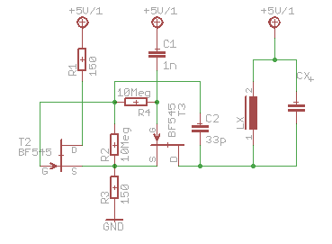
Picture 10: Broadband amplitude stabilized oscillator
Basically this is a 2 stage Franklin oscillator made with good available N-JFETs BF545A. The left transistor T2 works in common drain configuration, the right one T3 in common gate configuration.
To understand how it works let’s leave the two 10 MEG resistors R2 and R4 away for a moment and think about T2’s gate unconnected.
A signal on this gate will be amplified using an extremely low current as the amplifying unit is a FET. This NFET is a depletion type, so relative lower voltage will decrease the source drain current and therefore the source will move more to ground. This move is the input for T3 which is in a common base configuration as C1 grounds the base for AC current. Lower source potential on T3 means higher gate potential on T3 and therefore the T3 source drain current is increased. This higher current along LX and CX moves the drain of T2 more to ground.
The result is a 2 stage non inverting amplifier with extremely high input and low output resistance.
Now C2 feeds back the output of T3 to the gate of T2. Oscillation will start, but will not run into non linear behavior because of the special characteristic of J-NFETs.
Back to the two resistors R4 and R2. C2 is DC connected to 5 Volts through LX. With R2 it forms a low pass filter that creates a DC control voltage arriving from the amplitude oscillation at the source connection. This control voltage is also applied to T3 by R4. This is the amplitude stabilizing part of the oscillator.
Also the DUT is connected to the drain of T3 which makes it more reliable than other designs where the LC circuit is attached to a gate of FETs.
Lastly, if the source of T3 is disconnected from ground the drain will become a very high resistance to any other components. C2 is connected to other components by two 10 Meg resistors and by T2’s gate. The T2 gate does also have a very high resistance and low capacitance. The net is by disconnecting the source (or both sources) from ground it is possible to ‘free up’ the LC tuned circuit of LX and CX without leaving a relevant resistance in parallel to attenuate it.
In summary this design does serve all our requirements towards the oscillator at very low cost.
In the current LCQ-Meter design version 2.3 the oscillator works against a negative supply to measure LX and CX against ground (see full circuit diagram).
Super Fast Comparator Based Peak Detector
The peak detector for envelope measurement is the second challenging part of the overall design.
1. The peak detector has to ramp up to the input voltage very fast. Testing equations (17) and (18) with some quality Q values shows that measurements have to be done on a microseconds level. The expectation is a ramp up time of less than 1 microsecond.
2. The peak detector has to be on and off switchable to allow measurement at a specific time.
3. The peak detector has to store the momentary voltage long enough to get evaluated by the microcontroller which will take several microseconds.
4. The peak detector has to work with according accuracy and stability.
After a lot of research in literature and on the internet I did not find any design which will fit to those requirements. Most designs rely on operational amplifiers, some on comparators but all are much too slow. The fastest design achieved a settling time in milliseconds.
However, it can be done.
Picture 11 shows a ‘charge pump’ peak detector design based on the ultra fast 4.5 ns rail to rail comparator TLV3501 from Texas Instruments.
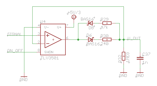
Picture 11: Comparator based peak detector
This comparator has the big advantage to provide a shutdown input which enables a switch on and off of the comparator within 100 ns. Furthermore it is a modern rail to rail type which allows measuring from ground up to the power supply level.
Here is how it works. Basically any positive voltage difference above a few mV between the positive and negative input of the comparator will result in a positive output (close to 5 V) on pin 6. A current through the fast diode D6 and R30 will quickly charge the holding capacitor C37.
As the negative input of the comparator is connected to that capacitor voltage level (closed loop) the charge will stop when the voltage level at C37 will reach the positive input level (the signal level).
If that input level is reached the comparator will toggle and the output on pin 6 will become negative (ground level). This will now discharge the holding capacitor slowly via R29 and D8.
If the signal level still increases or again increases another fast charge cycle will occur. If the signal level decreases C37 will slowly be discharged again via R29 and D8.
The net is the voltage on C37 will follow the positive signal peak level based on ultra fast charge cycles and much slower discharge cycles.
You may ask why are D8 and R29 needed at all, why is a (slower) discharge needed. This is because the comparator will overshoot due to switching delay time and needed hysteresis to prevent wild oscillation. In a real world the output voltage will go above the signal level and will stay there if no discharge will take place. This is also the reason why R30 cannot go much lower. R30 together with C37 form a low pass filter which mainly prevents that overshoot.
Only with a very careful selection of R30 and C37 the discharge way with R29 and D8 can be omitted. In the current LCQ-Meter design V2.3 this is the case, but pads for D8 and R29 are still on the PCB to allow further experimentation. Charge and discharge cycles can be widely adjusted by choosing different values for R30 and R29.
R14 is needed to discharge C7 after a measurement when the comparator is shut down which means the output goes to high resistance.
Please note not to take Schottky diodes in this design as their backward capacity is much higher which results in slower switching and more overshoot.
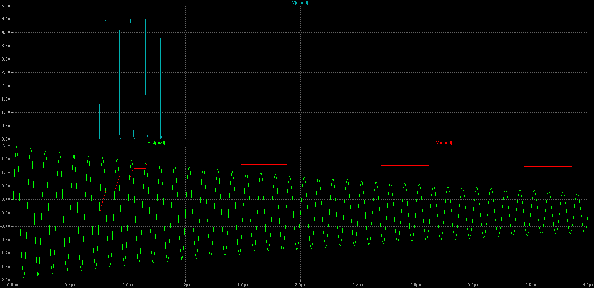
Going back to picture 8 the red line shows the voltage level across C37 after switching on the comparator.
The current design with R30 at 240 Ohm allows a ramp up time of less than 500nS. Someone could argue to reduce C37 to a lower value to achieve faster ramp up times. But this is not possible as the microcontroller charges its internal hold capacitor for the ADC converter via a relatively high resistance (see data sheet for the 16F1788). Also please remember that C37 is part of a low pass filter.
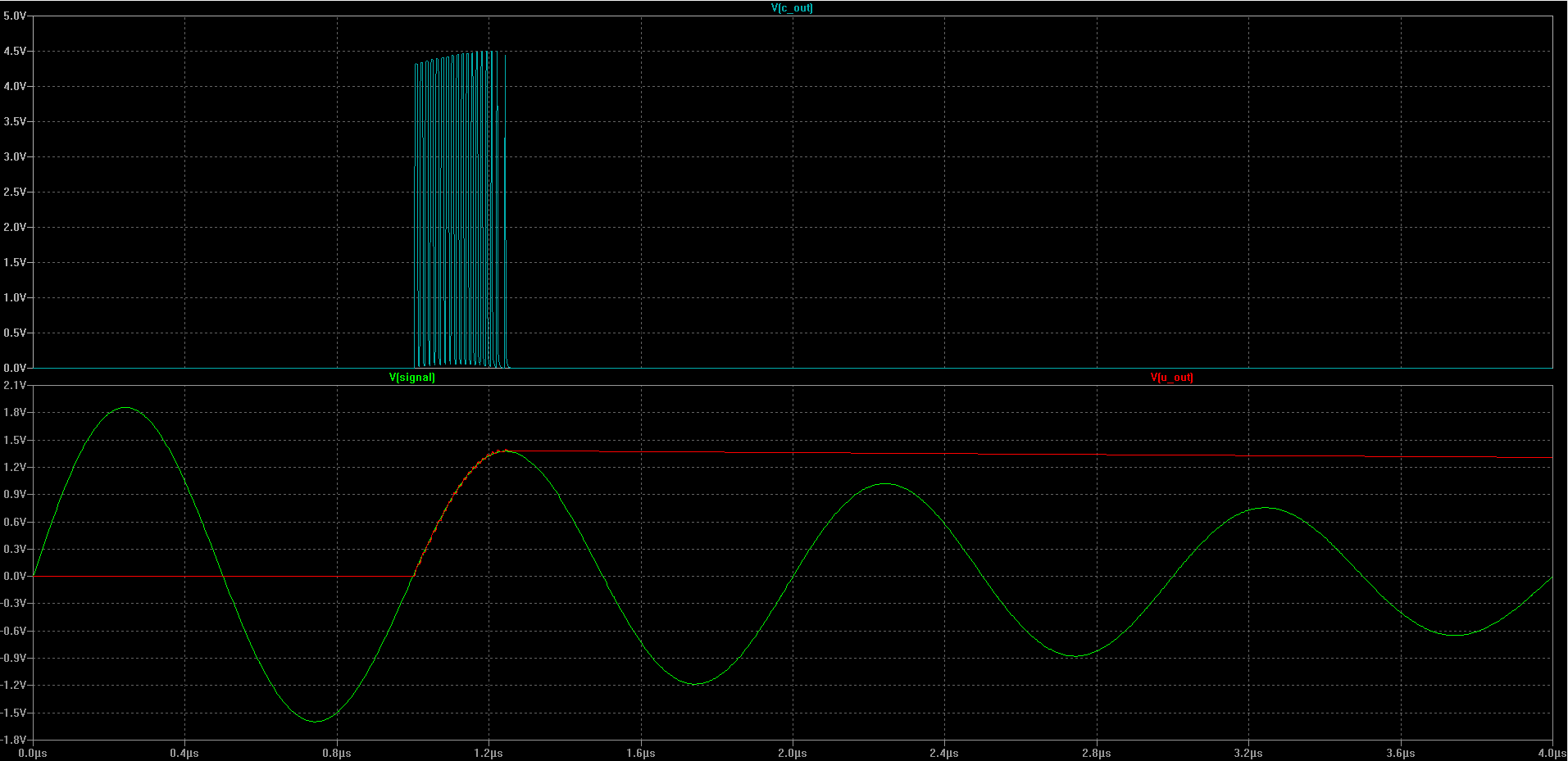
Picture 12: LTspice simulation of peak detector with signal at 1 MHz signal
Picture 12 shows an LTspice plot for this speed optimized design (as shown in picture 11) with an input signal at 1 MHz (green line), the voltage across the charging capacitor C37 (red line) and also the output voltage on the comparator pin (blue line).
The peak detector follows the signal until maximum which is the envelope at that time. If the peak voltage is measured not too far away from the recent peak, the digitized voltage will quiet closely represent the peak voltage of the envelope at that time.
A closer look to the comparator output voltage confirms that it is a series of very fast charge cycles.
Picture 13: LTSpice simulation of peak detector with signal at 10 MHz signal
The same plot with an input signal at 10 MHz is shown in picture 13. It can clearly be seen that the peak detector charges the holding capacitor during the maxima of the input signal towards the envelope voltage.
It takes about 500 nS until the envelope is reached. This raise time has to be incorporated into calculation of the envelope voltage at a defined time.
Putting It All Together
After discussing the details on the key components there is no much secret left on the rest of the design. Picture 14 shows the full circuit diagram.
The top middle part of the picture is the DUT Configuration Unit. It looks complex, but essentially it is about switching each needed tuned circuit configuration with 3 relays. Starting V2.3 latching relais are used to reduce power consumption. Analog switches cannot be used here as they have too much influence on the measurement in terms of residual resistance and stray capacitance. If one doesn’t need L and C measurement, just measurements on tuned circuits, all relays are not needed except one to switch on and off the 100 pF reference capacitor. The relays are controlled by the microcontroller using the transistor H-bridge matrix on the bottom right part of picture 14. Intentionally the H-bridges are implemented with discret components to save money compared to driver ICs.
On the left side there are some components to allow different supply voltage inputs. Either 5 Volts via a mini USB connector, an unregulated voltage 9 – 12 Volts via connector J1, or 3 – 4.5 Volts (2 - 3 cells) from batteries via connector JP2 can be used.
In practice it showed up that the USB supply voltage sometimes does contain a lot of quiet high noise. Therefore all sources are upwards converted to clean 5 Volts by the MCP1640 boost converter. However, in most cases and if battery supply is not needed the whole circuit can be driven by regulated 5 Volts directly which will save some components.
The TPS60403 charge pump creates a clean negative 5 Volt supply for the oscillator. This is needed as the DUT measurement should be against ground and there are no comparable PFET types to the NFET type BF545A easily available.
The supply of all key components of the circuit is decoupled via ferrite bears and bypassing capacitors to avoid any crosstalk through the supply lines.
The bottom left part shows the microcontroller, the LCD display and the user buttons. A cheap 16 letters 2 lines LCD display was used, but quality buttons for better handling and reliability.
There is an option to use an alternative, high quality 16 letters 2 lines LCD display from Electronic Assembly. Together with same or alternative buttons (Schurter) it can be assembled from the bottom of the PCB to have a very flat design to allow easy assembly into a case. For details see the bill of material.
The 16F1788 microcontroller used is a low price enhanced midrange type from Microchip. It is still 8 Bit, but includes large Flash ROM, RAM, EEPROM and some very nice analog components like comparators, operational amplifiers and also an asynchronous prescaler which allows frequency measurement up to at least 40 MHz.
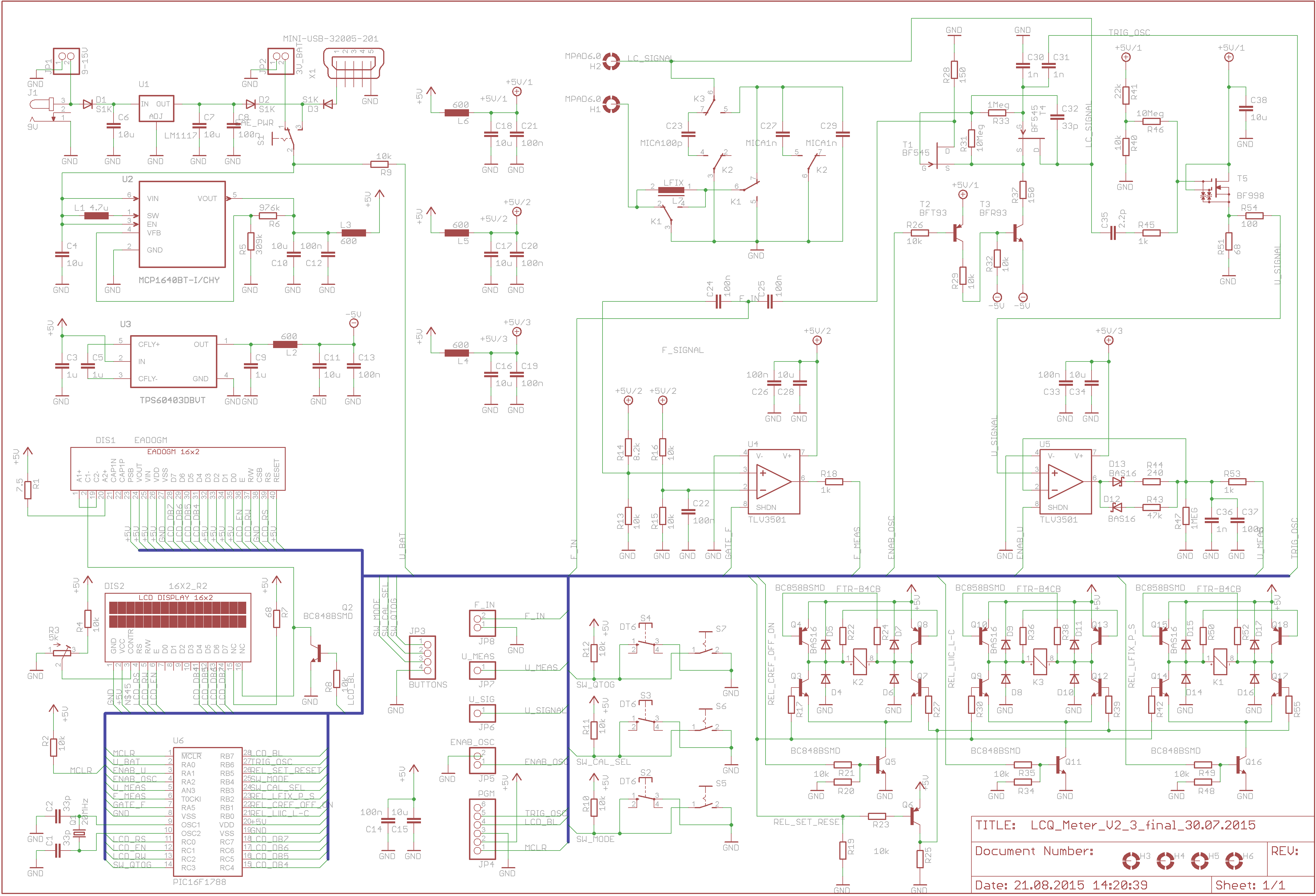
Picture 14: Circuit diagram
The top right part of picture 14 shows the oscillator as well as a buffer made with a dual gate MOSFET. This design is very often used in active probes as the input capacity is less than 2 pF and the input resistance is extremely high, at least at low to medium frequencies. The buffer is followed by the peak detector on the right middle part of the picture.
The middle of the picture includes another comparator to form clean square pulses for frequency measurement. The TLV3501 is a little bit oversized here, but as the microcontroller internal comparators cannot reach 30 MHz it was chosen to stay on these selected components.
The PCB layout version 2.3 before painting the ground plane is shown in picture 15. The size is exactly half of a Eurocard-Size. A double sided board is used with most components as SMD devices. I know that some HAMs are allergic against SMD, but it is definitely the better solution for such small designs at higher frequencies.
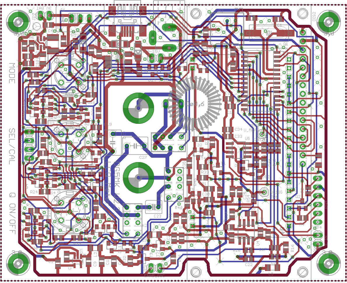
Picture 15: PCB layout
The good news is all components, except the TLV3501 and some of the power supply components, are also available as through the whole devices. So if someone would like to try without SMD it can be done. A previous prototype was build with through the whole devices with the size of a full Eurocard (picture 16).

Picture 16: LCQ-Meter with trough the whole components (mostly)
Picture 17 shows the bill of material.

Picture 17: Bill of Material